
The main research field is digital holographic microscopy systems suitable for high-precision, fast, real-time online detection of semiconductors and micro-optical devices, providing accurate measurement of three-dimensional morphology, and providing solutions and products for micro-nano processing and online detection in the semiconductor industry. The digital holographic microscope system will be able to improve online detection accuracy and simultaneously achieve real-time four-dimensional observation. It has extremely broad application scenarios in the field of high-precision detection in the manufacturing industry.
There are two types of microscopy systems: the reflective digital holographic microscopy system will be suitable for semiconductor detection, and the transmission digital holographic microscopy system will be suitable for thickness detection of micro-optical devices and biological samples. The application of digital holographic microscopy measurement is shown in Figure 9.1.

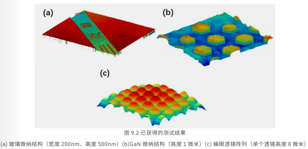
Obtained China Invention Authorization (2021.10), CN113219640A, a transmission-reflection digital holographic microscope system, and the obtained test results are shown in Figure 9.2.
Develop a machine-based digital holographic microscope suitable for laboratories, which can be used to test samples of specific sizes and achieve fast three-dimensional real-time imaging. At present, the laboratory has the conditions to build basic transmission and reflection digital microscopes. It is expected to complete the construction of two systems and conduct sample testing within half a year. At the same time, the phase recovery algorithm will be researched and improved. Combined with the problem needs of semiconductor and other industries, the machine should be miniaturized and compact, and online detection devices suitable for production line integration should be studied.
According to preliminary research results, the production lines of the semiconductor and display industries have a large number of testing needs. Among them, roughness, feature size, etc. have strict testing specifications and testing requirements. Currently, laboratory testing is the mainstay. Production line testing is mainly based on AOI testing equipment, which has low efficiency and low testing accuracy. Especially for photoresist testing, since the steps are inclined steps, it is easy to produce large errors. The digital holographic microscope can better solve the problems of step testing, error and test speed, and has a wide range of application scenarios.
Telephone:+86 755-23256198
Zip code:518118
Address:No. 3002, Lantian Road, Pingshan District, Shenzhen, Guangdong, China.

SZTU WeChat Public Account

SGIM WeChat Public Account
Copyright @SZTU